Tfmpage
  • Home
  • Transportation
  • Chemicals&Materials
  • Aerospace
  • Equipment
  • Energy
  • Technology
  • Electronics
  • Guest Post
No Result
View All Result
Get Started
Writy.
  • Home
  • Transportation
  • Chemicals&Materials
  • Aerospace
  • Equipment
  • Energy
  • Technology
  • Electronics
  • Guest Post
No Result
View All Result
Writy.
No Result
View All Result
P type Bismuth telluride doped Antimony 99.99% 200mesh Photoelectric material Bi0.5Sb1.5Te3 P Type Bi2Te3 powd

P type Bismuth telluride doped Antimony 99.99% 200mesh Photoelectric material Bi0.5Sb1.5Te3 P Type Bi2Te3 powd

2024-04-30
in Chemicals&Materials
Share on FacebookShare on Twitter

You might also like

The Unsung Hero of Modern Materials: Exploring the Power and Potential of Molybdenum Carbide Mo2C

The Unsung Hero of Modern Materials: Exploring the Power and Potential of Molybdenum Carbide Mo2C

2025-03-21
The Metal of Many Uses: Unveiling the Versatility and Innovation of Nickel Titanium nitinol material properties

The Metal of Many Uses: Unveiling the Versatility and Innovation of Nickel Titanium nitinol material properties

2025-03-21

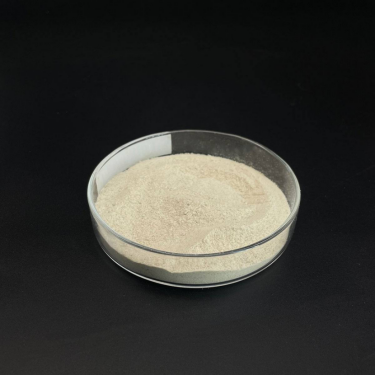
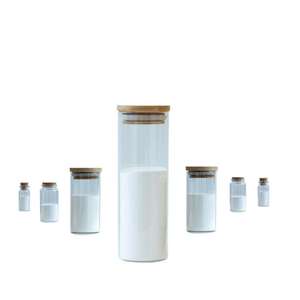
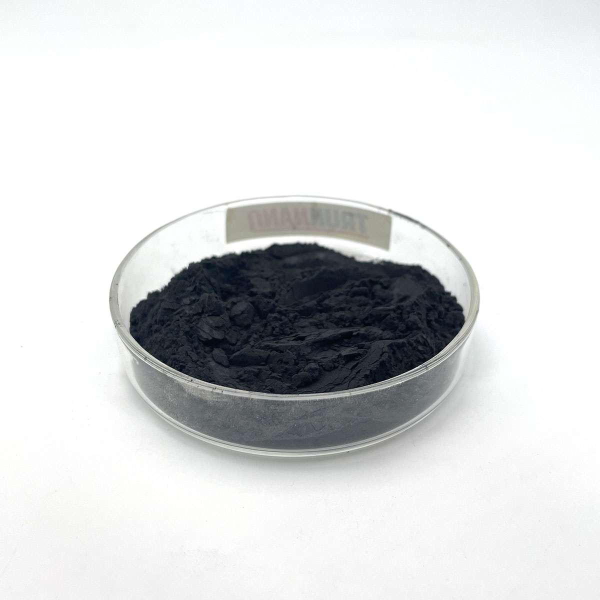
Overview of P type Bismuth telluride doped Antimony 99.99% 200mesh Photoelectric material Bi0.5Sb1.5Te3 P Type Bi2Te3 powd

Telluride and selenide compounds play a significant role in the field of semiconductors, particularly in the development of advanced electronic and optoelectronic devices. These materials belong to the chalcogenide family, characterized by their ability to form compounds with elements from groups IV-VI in the periodic table.


Tellurides: Compounds containing tellurium (Te) as the chalcogen. Examples include cadmium telluride (CdTe), mercury telluride (HgTe), and zinc telluride (ZnTe). These materials have found applications in solar cells, infrared detectors, and high-speed electronics due to their tunable bandgap, high electron mobility, and good thermal stability.


Selenides: Similar to tellurides, but with selenium (Se) replacing tellurium. Notable examples are cadmium selenide (CdSe), gallium selenide (GaSe), and zinc selenide (ZnSe). Selenide compounds are widely used in light-emitting diodes (LEDs), laser diodes, and solar cells due to their direct bandgap properties and efficient light absorption/emission capabilities.

Feature of P type Bismuth telluride doped Antimony 99.99% 200mesh Photoelectric material Bi0.5Sb1.5Te3 P Type Bi2Te3 powd

Direct Bandgap: Many telluride and selenide semiconductors have direct bandgaps, which facilitate efficient light emission and absorption processes. This makes them suitable for optoelectronic applications such as LEDs and lasers.


Tunable Bandgap: The bandgap of these materials can be adjusted by alloying or altering the composition (e.g., CdSe to CdTe), enabling customization for specific device requirements across a wide spectrum of wavelengths.


High Electron Mobility: Materials like HgCdTe exhibit high electron mobility, which is crucial for high-speed electronic devices and low-noise detector applications.


Thermal Stability: Some tellurides and selenides, like ZnTe and ZnSe, demonstrate good thermal stability, making them suitable for high-temperature operation and processing.


Non-Toxic Alternatives: With increasing environmental concerns, there’s a push towards exploring less toxic alternatives to commonly used semiconductors. For instance, Cd-based tellurides and selenides are being replaced or combined with less toxic elements like Mg or Mn in some applications.

P type Bismuth telluride doped Antimony 99.99% 200mesh Photoelectric material Bi0.5Sb1.5Te3 P Type Bi2Te3 powd

(P type Bismuth telluride doped Antimony 99.99% 200mesh Photoelectric material Bi0.5Sb1.5Te3 P Type Bi2Te3 powd)

Parameters of P type Bismuth telluride doped Antimony 99.99% 200mesh Photoelectric material Bi0.5Sb1.5Te3 P Type Bi2Te3 powd

Bismuth Telluride (Bi2Te3) is a promising material in the field of photovoltaics and optoelectronics due to its unique properties, such as high thermoelectric performance and sensitivity to light. Doping antimony (Sb) into Bi2Te3 can further enhance its characteristics, particularly when using high-purity Sb with a 99.99% purity level. In this case, we have a p-type Bi0.5Sb1.5Te3 compound, where the composition is intentionally engineered to achieve a p-type conductivity.

The material is processed into a fine powder form with a particle size of 200 mesh. This particle size is crucial for efficient light absorption and heat transfer, as smaller particles provide a larger surface area for interaction with incident photons. The 200-mesh powder ensures a consistent and uniform distribution, facilitating better integration in devices like photodiodes or thermoelectric generators.

The p-type doping introduces excess holes, which are positively charged carriers, making the material more susceptible to photoexcitation. These holes are generated when an electron from an impurity atom is knocked out, leaving behind a positive charge. This property enables the material to convert light directly into electrical current, a key characteristic for photovoltaic applications.

The bandgap of Bi0.5Sb1.5Te3 is essential for determining its optical response. By optimizing the Sb content, the bandgap can be tuned to capture a wide range of the solar spectrum, enhancing the efficiency of solar energy conversion. The precise stoichiometry also affects the material’s carrier mobility and lifetime, which are critical factors influencing the overall device performance.

In addition to its photovoltaic potential, Bi0.5Sb1.5Te3 exhibits good thermoelectric properties, allowing it to generate electricity from temperature differences. The combination of these two attributes makes it a sought-after material for waste heat recovery and portable power generation systems.

To summarize, the high-purity (99.99%) p-type Bi0.5Sb1.5Te3 photoelectric material with a 200-mesh powder composition offers exceptional properties for both photovoltaic and thermoelectric applications. Its fine particle size, tailored bandgap, and efficient carrier generation make it a competitive candidate for next-generation optoelectronic devices that harness light and convert it into useful electrical energy. Further research and development can lead to improved performance and widespread adoption in various industries, including renewable energy and electronic cooling technologies.

P type Bismuth telluride doped Antimony 99.99% 200mesh Photoelectric material Bi0.5Sb1.5Te3 P Type Bi2Te3 powd

(P type Bismuth telluride doped Antimony 99.99% 200mesh Photoelectric material Bi0.5Sb1.5Te3 P Type Bi2Te3 powd)

FAQ of Semiconductor Materials

What is the primary advantage of using P type Bismuth telluride doped Antimony 99.99% 200mesh Photoelectric material Bi0.5Sb1.5Te3 P Type Bi2Te3 powd?

Their primary advantages lie in their tunable bandgap, direct bandgap nature for efficient light interaction, and high electron mobility, which are essential for advanced optoelectronic and high-performance electronic devices.
Are P type Bismuth telluride doped Antimony 99.99% 200mesh Photoelectric material Bi0.5Sb1.5Te3 P Type Bi2Te3 powd compounds environmentally friendly?

While they offer excellent semiconductor properties, some telluride and selenide compounds, like those containing cadmium, pose environmental and health risks. Research is ongoing to develop more eco-friendly alternatives or to implement safe disposal methods.
How do P type Bismuth telluride doped Antimony 99.99% 200mesh Photoelectric material Bi0.5Sb1.5Te3 P Type Bi2Te3 powd compare to silicon in terms of performance?

Silicon is the most widely used semiconductor due to its abundance, stability, and well-established manufacturing processes. Telluride and selenide compounds, however, offer advantages in specific areas such as higher electron mobility, direct bandgap properties, and tunability, making them preferred for specialized applications like high-frequency electronics, photovoltaics, and infrared detection, where silicon falls short.
Can you grow high-quality single crystals of telluride and selenide semiconductors?

Yes, high-quality single crystals of these materials can be grown using techniques like Bridgman method, chemical vapor transport, or molecular beam epitaxy. Single crystals are desirable for many applications as they provide uniform electronic properties and reduced defects.

What are some future directions in the research of P type Bismuth telluride doped Antimony 99.99% 200mesh Photoelectric material Bi0.5Sb1.5Te3 P Type Bi2Te3 powd?

Future research directions include developing new materials with improved performance and reduced toxicity, enhancing device efficiency and scalability, exploring novel device architectures like 2D materials and quantum dots, and integrating these materials into next-generation technologies such as flexible electronics, quantum computing, and advanced sensor systems.

Inquiry us


    Tags: bismuth telluride

    Related Stories

    The Unsung Hero of Modern Materials: Exploring the Power and Potential of Molybdenum Carbide Mo2C

    The Unsung Hero of Modern Materials: Exploring the Power and Potential of Molybdenum Carbide Mo2C

    2025-03-21
    0

    Intro to Molybdenum Carbide Molybdenum carbide is an amazing product. It has one-of-a-kind residential or commercial properties that make it...

    The Metal of Many Uses: Unveiling the Versatility and Innovation of Nickel Titanium nitinol material properties

    The Metal of Many Uses: Unveiling the Versatility and Innovation of Nickel Titanium nitinol material properties

    2025-03-21
    0

    Intro to Nickel Titanium Nickel titanium, also called Nitinol, is a special alloy. It has special homes that make it...

    The Silver Solution: Unveiling the Power of Nanosilver Solutions colloidal silver walgreens

    The Silver Solution: Unveiling the Power of Nanosilver Solutions colloidal silver walgreens

    2025-03-20
    0

    Intro to Nanosilver Solutions Nanosilver services are acquiring interest because of their unique homes. These options consist of tiny bits...

    Tantalum Carbide Powder: A Material of the Future tantalum carbide price

    Tantalum Carbide Powder: A Material of the Future tantalum carbide price

    2025-03-18
    0

    Intro to Tantalum Carbide Powder Tantalum carbide powder is a special product used in lots of markets. It is recognized...

    Next Post
    Supply 99.999% Sb2Te3 Antimony Telluride

    Supply 99.999% Sb2Te3 Antimony Telluride

    About Tfmpage

    The Tfmpage website is for desi entertainment lovers across India, USA and UK. We often cover breaking News & Trending topics in India and have been referenced by numerous media outlets. Follow us on our Social media profiles for the latest updates and news.

    No Result
    View All Result
    • Landing Page
    • Buy JNews
    • Support Forum
    • Pre-sale Question
    • Contact Us