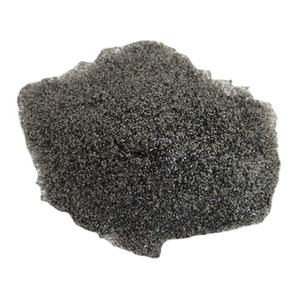
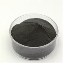
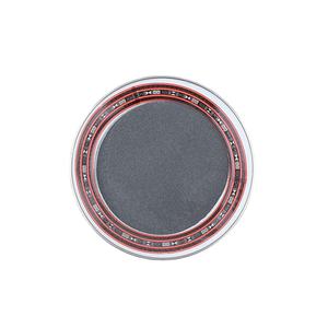
Overview of Sb2Te3 Antimony telluride sputtering target thin film coating material semiconductor
Telluride and selenide compounds play a significant role in the field of semiconductors, particularly in the development of advanced electronic and optoelectronic devices. These materials belong to the chalcogenide family, characterized by their ability to form compounds with elements from groups IV-VI in the periodic table.
Tellurides: Compounds containing tellurium (Te) as the chalcogen. Examples include cadmium telluride (CdTe), mercury telluride (HgTe), and zinc telluride (ZnTe). These materials have found applications in solar cells, infrared detectors, and high-speed electronics due to their tunable bandgap, high electron mobility, and good thermal stability.
Selenides: Similar to tellurides, but with selenium (Se) replacing tellurium. Notable examples are cadmium selenide (CdSe), gallium selenide (GaSe), and zinc selenide (ZnSe). Selenide compounds are widely used in light-emitting diodes (LEDs), laser diodes, and solar cells due to their direct bandgap properties and efficient light absorption/emission capabilities.
Feature of Sb2Te3 Antimony telluride sputtering target thin film coating material semiconductor
Direct Bandgap: Many telluride and selenide semiconductors have direct bandgaps, which facilitate efficient light emission and absorption processes. This makes them suitable for optoelectronic applications such as LEDs and lasers.
Tunable Bandgap: The bandgap of these materials can be adjusted by alloying or altering the composition (e.g., CdSe to CdTe), enabling customization for specific device requirements across a wide spectrum of wavelengths.
High Electron Mobility: Materials like HgCdTe exhibit high electron mobility, which is crucial for high-speed electronic devices and low-noise detector applications.
Thermal Stability: Some tellurides and selenides, like ZnTe and ZnSe, demonstrate good thermal stability, making them suitable for high-temperature operation and processing.
Non-Toxic Alternatives: With increasing environmental concerns, there’s a push towards exploring less toxic alternatives to commonly used semiconductors. For instance, Cd-based tellurides and selenides are being replaced or combined with less toxic elements like Mg or Mn in some applications.
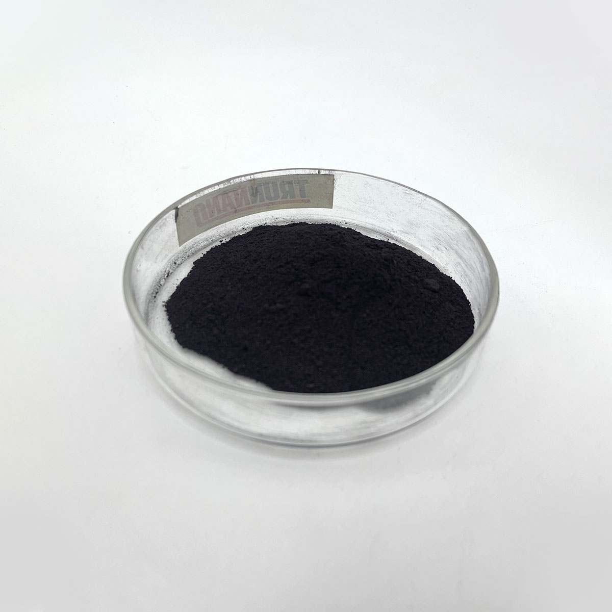
(Sb2Te3 Antimony telluride sputtering target thin film coating material semiconductor)
Parameters of Sb2Te3 Antimony telluride sputtering target thin film coating material semiconductor
Antimony Telluride (Sb2Te3), also known as antimony trisulfide, is a fascinating material with a myriad of applications in the realm of semiconductors and thin film coatings. It has gained significant attention due to its unique properties that make it suitable for various technological advancements, particularly in the fields of optoelectronics, thermoelectrics, and spintronics.
Firstly, Sb2Te3 is a chalcogenide semiconductor, meaning it belongs to the group of materials that incorporate sulfur or selenium along with metal elements. Its bandgap falls within the mid-infrared range, typically around 0.2 to 0.3 eV, which allows for efficient absorption of light at wavelengths beyond those of silicon-based semiconductors. This makes it an attractive candidate for infrared photodetectors and optical modulators.
In the context of thin film coatings, Sb2Te3 offers excellent thermal stability and high reflectivity, making it a popular choice for thermally stable mirrors and coatings for solar cells. The material’s ability to change its optical properties upon temperature variations can be exploited in thermochromic devices, where the appearance of a surface changes color based on temperature.
Another crucial aspect of Sb2Te3 is its high thermoelectric performance. It possesses a high Seebeck coefficient, which is a measure of the voltage generated per unit temperature difference across the material. This property enables the development of thermoelectric generators and coolers, converting waste heat into electricity or vice versa. Sb2Te3 thin films can be integrated into microscale devices for efficient power generation or waste heat management.
Furthermore, Sb2Te3 exhibits strong spin-orbit coupling, which is the interaction between an electron’s spin and its motion. This feature is essential for spintronics, a field that exploits the spin of electrons for information processing. The material can be used to create spintronic devices like magnetic memory and logic elements, offering potential advantages over traditional charge-based electronics in terms of energy efficiency and data storage density.
The synthesis of Sb2Te3 thin films can be achieved through various deposition techniques, including sputtering, chemical vapor deposition (CVD), and molecular beam epitaxy (MBE). Sputtering, in particular, is a widely employed method due to its simplicity and scalability. During sputtering, high-energy ions bombard a target containing Sb and Te, releasing atoms that adhere to a substrate, forming a uniform thin film. The process can be controlled to optimize film properties, such as thickness, crystallinity, and stoichiometry.
However, it is worth noting that Sb2Te3 thin films can pose challenges in terms of device fabrication, as the material is sensitive to defects and oxidation. To overcome these issues, researchers often employ post-deposition treatments, such as annealing or encapsulation, to improve film quality and device performance.
In summary, Sb2Te3 is a versatile semiconductor material with unique properties that make it suitable for a wide range of applications in thin film coatings and advanced electronic devices. Its optical, thermoelectric, and spintronic capabilities, combined with the possibility of scalable deposition methods like sputtering, position it as a promising material for future technological innovations. However, further research and optimization are necessary to fully harness its potential and address the challenges associated with its use in practical devices.
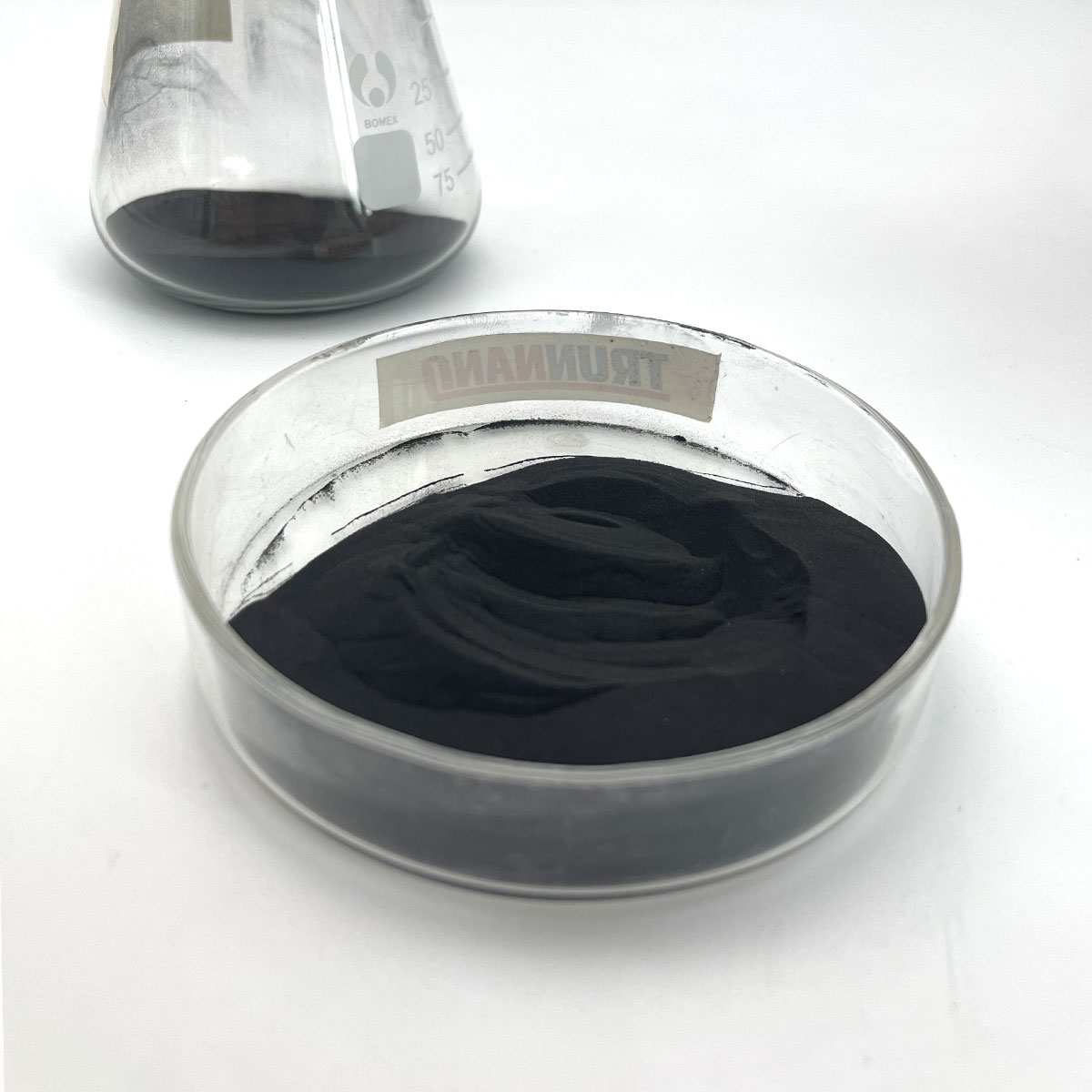
(Sb2Te3 Antimony telluride sputtering target thin film coating material semiconductor)
FAQ of Semiconductor Materials
Inquiry us

